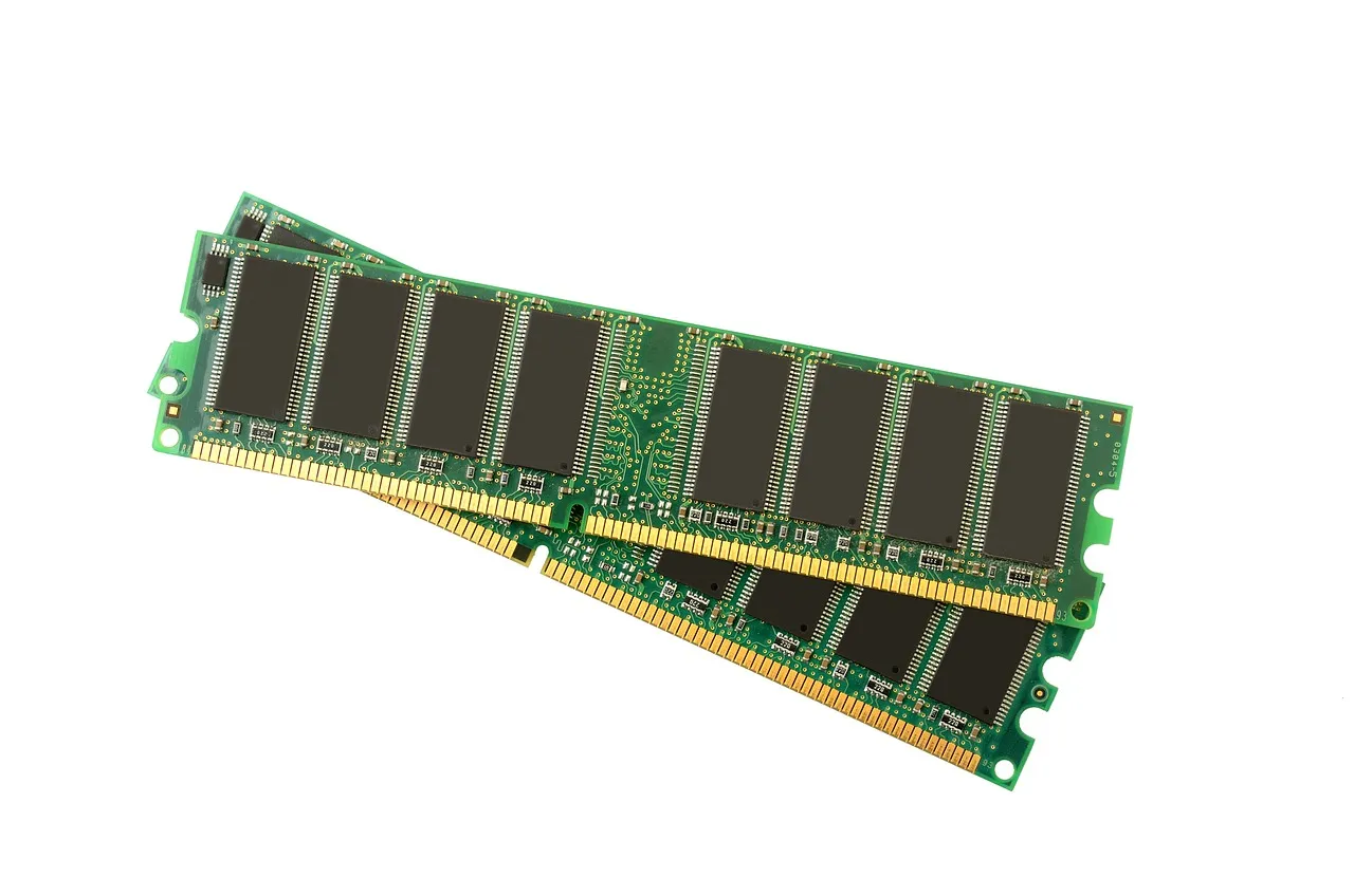
STANFORD, 27 AUG 2026 — Samsung has shown LPDDR5X-PIM, low-power memory with arithmetic units built into the DRAM itself. On a Llama 3.1 8B workload it reported 2.28 times faster model run time and 3.01 times the tokens per second against conventional LPDDR5X.
The headline figure is an eight-times bandwidth jump, from 76.8 GB/s to 614 GB/s. The number is real, and it is not measured on the memory bus.
The eight times is inside the memory, not on the bus
614 GB/s is the bandwidth available to the compute units sitting inside the DRAM. It is not the speed at which the memory talks to the processor.
The external interface is still LPDDR5X, operating at its normal rate. Nothing about this part makes the connection between memory and host faster, and a device that reads data out of it in the ordinary way sees exactly the performance it saw before.
That is not a caveat undermining the technology. It is the whole point of it. Processing in memory works by not moving the data at all — performing the arithmetic where the bits already are, in the wide internal paths that DRAM has always had internally and never exposed. The eight-times figure describes the width of a road inside a building, not the road leading to it.
Coverage saying the memory is eight times faster has described something that would be a different and much less interesting product.
Why moving the data is the expensive part
The premise of in-memory processing is an awkward fact about modern computing. Fetching a number from memory costs far more energy than the arithmetic performed on it once it arrives.
For a language model that ratio is brutal. Generating each token requires reading the model's weights, and the processor spends most of its time waiting for them rather than computing. We made this point about mobile silicon when Xiaomi shipped the first phone chip supporting LPDDR6: on-device inference is bounded by how fast weights arrive, not by how many cores are available to receive them.
Faster memory standards attack that by widening the road. Processing in memory attacks it by not making the journey. For the operations it can handle, the weights never leave the chip they are stored on, and the energy and time spent on the trip simply do not occur.
The standard package is the point
The specification detail that matters commercially is the least exciting one. This is a JEDEC-standard 561-ball package, 16GB across four dies per rank, in two 64-bit ranks.
That means it fits where LPDDR5X fits. A device maker adopting it is not redesigning a board, negotiating a new socket or waiting for an ecosystem to form around a novel interface — the reasons most memory-architecture research never reaches a product.
The history of processing in memory is largely a history of good ideas that required everyone else to change first. Putting one in a standard package is what turns a research direction into a component a phone maker can actually order. That decision matters more than any of the performance figures.
What it cannot do
The in-memory units perform a limited set of operations. This is not a general-purpose processor that happens to live in the DRAM. It is arithmetic hardware built for the repetitive patterns that dominate inference.
Samsung describes this as the first low-power PIM part with multi-precision data type support, which widens the range of models it can serve usefully. It does not make it general. Anything the in-memory units cannot do still travels to the accelerator over the ordinary interface at the ordinary speed.
So the 3.01 times figure is a measurement of one model, of one size, on one edge accelerator. A workload whose bottleneck sits elsewhere will see a fraction of that, and a workload dominated by operations the units do not implement will see close to none. The speedup is real and it is a measurement of that model. It should not be expected to generalise.
Logic in a memory process is harder than it sounds
Processing in memory has been discussed for decades and has shipped rarely. The reason is manufacturing rather than architecture.
DRAM and logic are built on processes optimised for opposite things. A memory process is tuned to pack storage cells as densely and cheaply as possible; a logic process is tuned for fast, low-leakage transistors. Building arithmetic units on a DRAM line means accepting transistors that are slower and less efficient than the same circuit would be on a logic process, and spending die area that would otherwise have held storage.
So every in-memory compute unit costs capacity and yield. That trade only pays when the operation it performs would otherwise have required moving a great deal of data, which is exactly the case for inference and was not the case for the general-purpose workloads earlier PIM proposals targeted.
The second constraint is heat. A DRAM package is designed to dissipate very little, because memory has historically done very little work. Adding computation adds power draw inside a component with no heatsink, and in a phone — a sealed chassis with no fan — that budget is small and already spent. How much of the reported gain survives in a thermally constrained device, sustained rather than in a burst, is the question a datasheet will answer and a conference slide does not.
Where this sits against HBM
Samsung is explicit that this complements high-bandwidth memory rather than replacing it, and the division is sensible.
HBM remains the answer where power and cost are secondary to raw bandwidth, which describes a training cluster. It is also expensive and supply-constrained, with HBM4 quoted around US$550 a stack, and that cost is precisely why an alternative for inference is attractive.
LPDDR5X-PIM targets the other end: phones, laptops, edge boxes and the servers where efficiency matters more than peak throughput. Those are also, by volume, most of the computers in the world, and inference is migrating toward them.
What it means from here
For anyone building products that run models locally in this region, the practical signal is about where to expect the next capability jump.
The assumption has been that on-device AI improves when the processor improves, so the roadmap to watch is the accelerator's. This suggests the memory roadmap matters at least as much, and possibly more, because the constraint was never the arithmetic.
Silicon suppliers should now be asked about the memory subsystem rather than only about neural engine performance. Does it handle any of the inference work, and what does the device do when a model's weights exceed what will fit?
Nothing here has shipped in a product yet, and a conference presentation is a statement of intent as much as of capability. What has changed is that the least-examined component in the device has become one of the more interesting ones.

View author profile → · Editorial policy