TOKYO, 11 AUG 2026 — Sony and TSMC are reported to be putting about ¥1 trillion into a joint venture making image sensors in Kumamoto, and the interesting part is not the camera in your phone. It is what they say the sensors are for.
Nikkei reported on 10 August that the two companies will spend roughly ¥1 trillion, about US$6.32 billion, on next-generation image-sensor chips. The venture is to be owned around 60% by Sony and 40% by TSMC, with commercial production starting as early as 2029 at Sony Semiconductor Solutions' existing plant in Koshi, Kumamoto prefecture.
Two leaders in different things
Sony is the world's largest image-sensor maker, its position built on sensor design: pixel structures, stacking, and the analogue engineering that turns light into usable signal. TSMC, the largest contract chipmaker, leads on process technology.
Image sensors have historically been made on trailing-edge processes, because a photodiode does not benefit from a smaller transistor the way a processor does. But a modern sensor is more than a photodiode array. It is a stack, with logic and memory bonded underneath the pixels. That logic layer benefits from the density and power efficiency of a modern process, which allows on-sensor computation before the data is sent elsewhere.
That is the joint in this joint venture. Sony knows what the sensor should do; the improvement now available comes from the layer underneath it, and TSMC makes that layer better than anyone.
The reason is robots, and they have said so
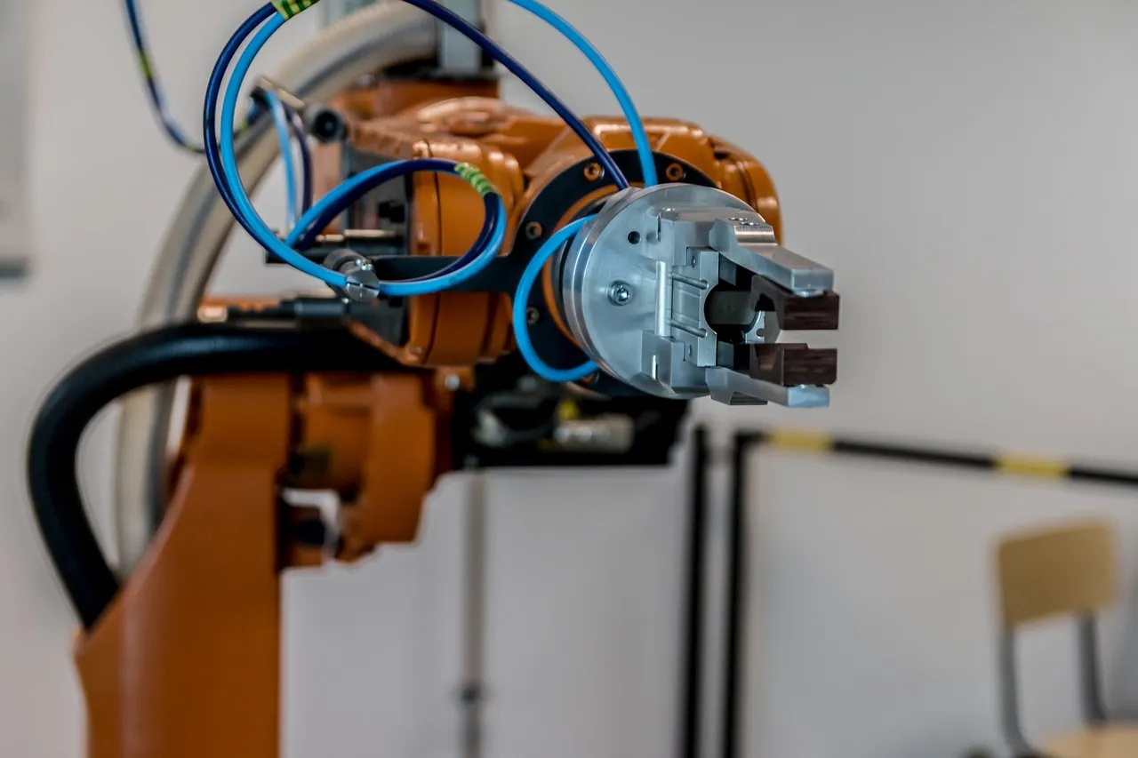
When the two companies announced their intention to work together in May, they said the partnership would explore physical AI — automotive and robotics.
That framing should be taken at face value, not as marketing; it explains a decision that would otherwise look odd. Smartphone volumes are flat and the sensor competition there is mature. A ¥1 trillion investment for a 2029 production start only pays back if you are betting on a market that does not exist yet at scale: machines that move through the physical world and need to see it.
What that market needs from a sensor is different from what a phone needs. Not just resolution, but low latency, high dynamic range for a vehicle coming out of a tunnel, reliability across temperature, functional-safety qualification, and processing close to the pixel so a robot is not shipping raw frames to a GPU and waiting. [Sentence deleted]
Where this sits in the map
Kumamoto is not a random choice. TSMC already runs Japan Advanced Semiconductor Manufacturing there, the venture with Sony and Denso that opened Japan's most prominent recent fab, and the prefecture now has the supply chain, the water and the trained people that a second facility can draw on.
It also fits a pattern we have been tracking in the region all year, where the most interesting semiconductor investment is shifting from general-purpose logic to application-specific silicon. In the last week alone we have covered AMD buying a company that builds a chip to run one model. A sensor fab dedicated to physical AI is the same instinct with a longer horizon and a factory attached.
Why 2029 is both far away and not
Three years feels slow against the pace of AI announcements and is normal for a fab. Site preparation, tool installation, qualification and yield ramp do not compress, and a sensor line qualified for automotive use has to clear reliability standards that consumer parts never face.
Set that against the customer timeline and it looks better judged. Vehicles being designed now ship around then; humanoid and warehouse robotics programmes currently in pilot reach volume in roughly the same window. A part that arrived in 2027 would be early for the design wins it is aimed at, and one arriving in 2031 would be late.
The risk in the middle is demand, not schedule. If physical AI grows more slowly than the current spending implies, this is a very large sensor line pointed at a market that is still mostly forecast, and image-sensor demand from smartphones is not going to absorb the difference.
The competitive picture
Sony has a long-standing lead in image sensors, and its position is strongest in the high end where design sophistication matters most. Samsung competes seriously in mobile and has its own fabs; OmniVision is a substantial presence in automotive; Chinese suppliers have been moving up through the volume segments for several years.
None of them has an obvious, committed leading-edge partner for the logic layer. That is what this venture buys. If the physical-AI thesis is right, it is a structural advantage, not just a product advantage — one that would take competitors years and significant capital to replicate.
What to hold lightly
This is a Nikkei report, not a joint announcement. Reuters and others have carried it as Nikkei's reporting, which is how we are carrying it too. The May statement of intent is on the record; the figure, the ownership split and the 2029 date are not, as far as we can establish, confirmed by either company.
That matters for the parts most likely to be quoted. A number like ¥1 trillion travels well and hardens fast, and a plan for 2029 is a plan, not a commitment. Both companies have every commercial reason not to confirm the detail yet.
What to watch
Whether Sony and TSMC confirm the terms, and whether the ownership split survives to the definitive agreement. The 60/40 structure indicates who is expected to lead the technology, making it the most informative figure in the report.
Whether Japanese government support appears. The Kumamoto fabs have been supported before, and a physical-AI sensor line fits the stated industrial policy closely enough that its absence would be more surprising than its presence.
And whether anybody else moves on sensors for robotics. Sony's lead in image sensors is large, but a 2029 production start is a long time to leave a signal that visible on the table.